

Odisha CM laid the foundation stone for advanced 3D chip packaging facility in Bhubaneswar

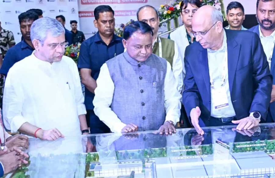
India has taken a step forward towards its semiconductor ambitions. The foundation stone for the country’s first advanced 3D chip packaging facility was laid in Bhubaneswar. The project represents a significant milestone in strengthening the domestic semiconductor ecosystem and aligns with the broader vision of Atmanirbhar Bharat in high-end electronics manufacturing.
Addressing the event, Chief Minister Mohan Majhi described the initiative as a historic achievement for both the state and the nation. He noted that this is the first time an advanced 3D glass solutions semiconductor project is being established in India, positioning Odisha at the forefront of next-generation technology infrastructure.
He also highlighted that global technology leaders such as Intel, Lockheed Martin, and Applied Materials are closely associated with advanced packaging technologies. Their growing interest reflects Odisha’s emergence as a promising industrial destination.
Providing further details, the Chief Minister said the project involves an investment of nearly Rs 2,000 crore. Once operational, the facility is expected to manufacture around 70,000 glass panels annually, along with 50 million assembled units and approximately 13,000 advanced 3D heterogeneous integration (3DHI) modules.
He further underscored that Odisha is uniquely positioned as the only state in India hosting both the country’s first compound semiconductor fabrication unit and its first 3D glass substrate packaging facility.
The initiative is expected to create significant employment opportunities, attract additional investments, and accelerate Odisha’s rise as a key hub in India’s semiconductor and electronics manufacturing landscape.

See What’s Next in Tech With the Fast Forward Newsletter


Tweets From @varindiamag
Nothing to see here - yet
When they Tweet, their Tweets will show up here.