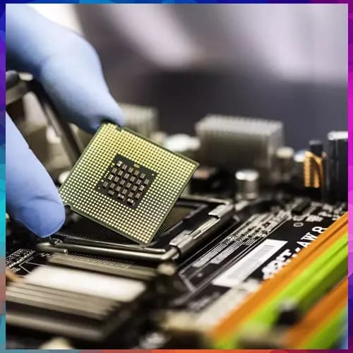

Samsung Electronics unveiled a new generation of AI memory technologies on Tuesday, introducing advances in NAND and high-bandwidth memory (HBM) architectures aimed at addressing the growing storage and performance demands of AI inference workloads.
The company showcased its latest memory roadmap at the Future of Memory and Storage (FMS) 2026 conference in Santa Clara, California, where it introduced a prototype of its V10 Bonding V-NAND (BV-NAND) technology and outlined new concepts for vertically stacked high-bandwidth memory.
Samsung said its BV-NAND prototype uses a new wafer-bonding architecture with more than 400 memory layers, increasing storage density by about 58% compared with its previous V9 NAND technology while improving read, write and input/output performance.
The company said the technology is designed to meet growing demand for higher-capacity, more power-efficient storage as AI workloads increasingly shift from model training to inference, where systems must rapidly retrieve and process vast amounts of data.
Samsung also unveiled concept designs for what it described as the industry's first zHBM and zNAND-O architectures, representing its vision for future AI memory systems.
Unlike conventional HBM, which is positioned alongside AI processors, zHBM places memory vertically above AI accelerators, reducing the distance data travels between memory and compute. Samsung said the architecture has the potential to significantly increase bandwidth while improving energy efficiency and reducing heat generation.
According to the company, its wafer-bonding approach could ultimately deliver more than 10 times the memory density of conventional HBM5 technology, triple energy efficiency and reduce thermal resistance by more than half.
The announcements reflect the semiconductor industry's growing focus on memory architectures tailored for AI inference, where the ability to move and access large volumes of data efficiently is becoming as important as raw computing performance.
Samsung's latest technology roadmap comes as demand for AI memory continues to outpace broader semiconductor markets. The company said last week that long-term agreements with major customers are expected to account for 60% to 70% of its memory production capacity over the longer term, underscoring sustained investment by hyperscalers in AI infrastructure.
The introduction of new memory technologies also highlights the industry's search for alternatives beyond conventional HBM as AI models become larger and increasingly memory-intensive. By combining higher-density NAND with new three-dimensional memory architectures, Samsung aims to improve both storage capacity and energy efficiency for next-generation AI servers and accelerators.
Commercial availability and production timelines for the newly announced technologies were not disclosed.
The company showcased its latest memory roadmap at the Future of Memory and Storage (FMS) 2026 conference in Santa Clara, California, where it introduced a prototype of its V10 Bonding V-NAND (BV-NAND) technology and outlined new concepts for vertically stacked high-bandwidth memory.
Samsung said its BV-NAND prototype uses a new wafer-bonding architecture with more than 400 memory layers, increasing storage density by about 58% compared with its previous V9 NAND technology while improving read, write and input/output performance.
The company said the technology is designed to meet growing demand for higher-capacity, more power-efficient storage as AI workloads increasingly shift from model training to inference, where systems must rapidly retrieve and process vast amounts of data.
Samsung also unveiled concept designs for what it described as the industry's first zHBM and zNAND-O architectures, representing its vision for future AI memory systems.
Unlike conventional HBM, which is positioned alongside AI processors, zHBM places memory vertically above AI accelerators, reducing the distance data travels between memory and compute. Samsung said the architecture has the potential to significantly increase bandwidth while improving energy efficiency and reducing heat generation.
According to the company, its wafer-bonding approach could ultimately deliver more than 10 times the memory density of conventional HBM5 technology, triple energy efficiency and reduce thermal resistance by more than half.
The announcements reflect the semiconductor industry's growing focus on memory architectures tailored for AI inference, where the ability to move and access large volumes of data efficiently is becoming as important as raw computing performance.
Samsung's latest technology roadmap comes as demand for AI memory continues to outpace broader semiconductor markets. The company said last week that long-term agreements with major customers are expected to account for 60% to 70% of its memory production capacity over the longer term, underscoring sustained investment by hyperscalers in AI infrastructure.
The introduction of new memory technologies also highlights the industry's search for alternatives beyond conventional HBM as AI models become larger and increasingly memory-intensive. By combining higher-density NAND with new three-dimensional memory architectures, Samsung aims to improve both storage capacity and energy efficiency for next-generation AI servers and accelerators.
Commercial availability and production timelines for the newly announced technologies were not disclosed.